Building an 8-Bit CPU on a Breadboard
Years ago I came upon Ben Eater’s series of YouTube videos about building an 8-bit computer on a series of breadboards. I watched the entire series but didn’t have the energy to complete the project myself. Then a few months ago I decided to finally give it a go.
After toiling away with wires for around three months, spending way too much money, and starting over twice, I finally completed my modified build of Ben’s computer (which is the SAP-1 from the book Digital Computer Electronics by Albert Paul Malvino).
First Build
I first started the project building it exactly as Ben does in the videos and I got pretty far until I hit a problem that most everyone does who starts this project: sporadic issues. Things like signal noise and power distribution troubles. No one is quite sure how Ben managed to avoid encountering them.
It was around when I started adding the program counter in my first build that I began to have issues. My counter was counting twice for every clock tick. And some other things were acting strangely and unpredictably. It turned out to be a couple of different issues.
Bad Power Distribution
The original design has power input going to one of the breadboards and then power is daisy chained to all of the others. The chips farthest away from the power input received lower voltages than the closest chips, sometimes even dipping below the recommended voltage levels of the chips.
Floating Chip Pins
The original design uses 74LS TTL chips which, it turns out, should never have their input pins floating. Instead you should tie either low or high. It doesn’t really matter which; what’s important is that the inputs aren’t floating somewhere in between. Although I did read that for lowest power distribution you should tie the inputs to whatever will cause the outputs to be high. For example, an AND gate should have both inputs tied high while a NOT gate should have its input tied low.
Lack of Bypass Capacitors
The original design used capacitors only for achieving specific timing with the 555 chips. It is commonly recommended when designing circuits to place small capacitors (called decoupling/bypass caps) near the power pins of integrated circuits (like the 74LS chips) to help smooth out power line noise. If the voltage has a spike the capacitor will absorb it and if the voltage drops the capacitor will provide enough to keep the voltage to the chip stables.
Here’s an example of the original clock module I built which has the issue of floating chip pins and a lack of capacitors near the power pins.
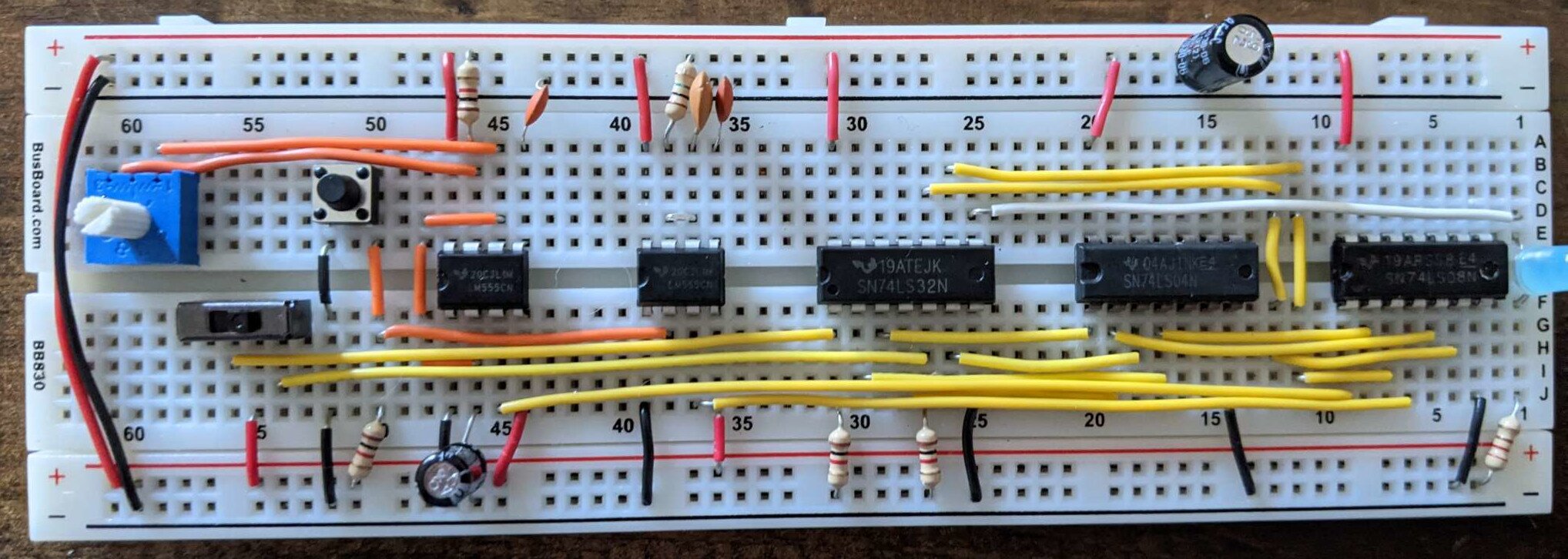
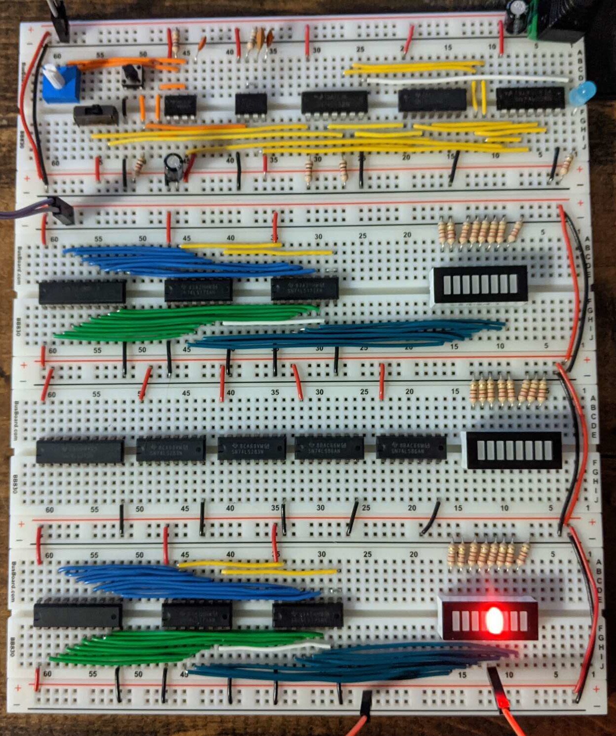
Here’s my original build of the A/B/ALU modules where you can see the daisy-chaining down the right side, with the power input in the upper-right corner.
I did make some modifications from Ben’s design from the beginning, mainly concerning LEDs. The original design often connected LEDs directly to output pins of the chips because the 74LS chips have internal resistors on the outputs. That’s technically okay but can lead to subtle troubles that are hard to find. It was drilled into me long ago that you always put current-limiting resistors on LEDs so that’s what I did.
I also used LED bars because I found it annoying trying to line up individual LEDs in a row that looked clean. I also think the bars look really cool.
Second Build
When I started seeing unpredictable behavior (a terrifying concept), I decided to start over and rebuild. I could have made the modifications in-place but it would have been annoying, and I’m more of a burn-it-and-start-anew kind of person anyway.
I decided to start over, addressing the floating inputs and lack of bypass capacitors, as well as another idea I had.
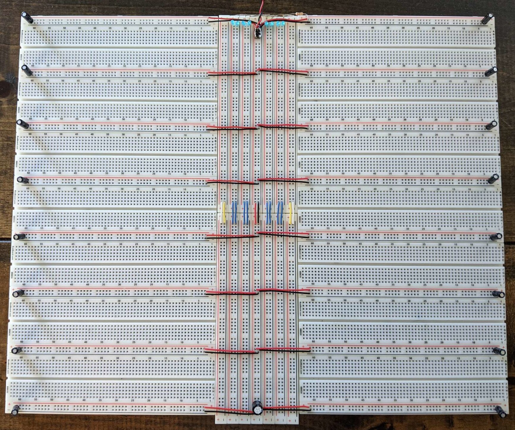
Central Reset and Clock Lines
In addition to fixing the problems I had in the first build, I also wanted to fix the problem of messy wiring. I had the idea to add four extra lines down the center next to the bus: two clock, one reset, and one inverted reset. The reset and clock lines go to nearly every module so it was much cleaner this way.
Here is the rebuilt clock module which demonstrates all of the changes:
I went a bit overboard and starting putting the bypass capacitors right next to the ICs which ended up eating precious breadboard space. It became increasingly annoying because it was no hard to route wires in between the chips.
Third Build
I had nearly everything wired up and in place when I decided to start over yet again. I had some new ideas (again) and I wanted to start clean rather than try to modify in-place. Why do I do this to myself?
74HC Chips
The 74HC chips are CMOS instead of TTL and consume (a lot) less power as a result. They also tend to be less noisy.
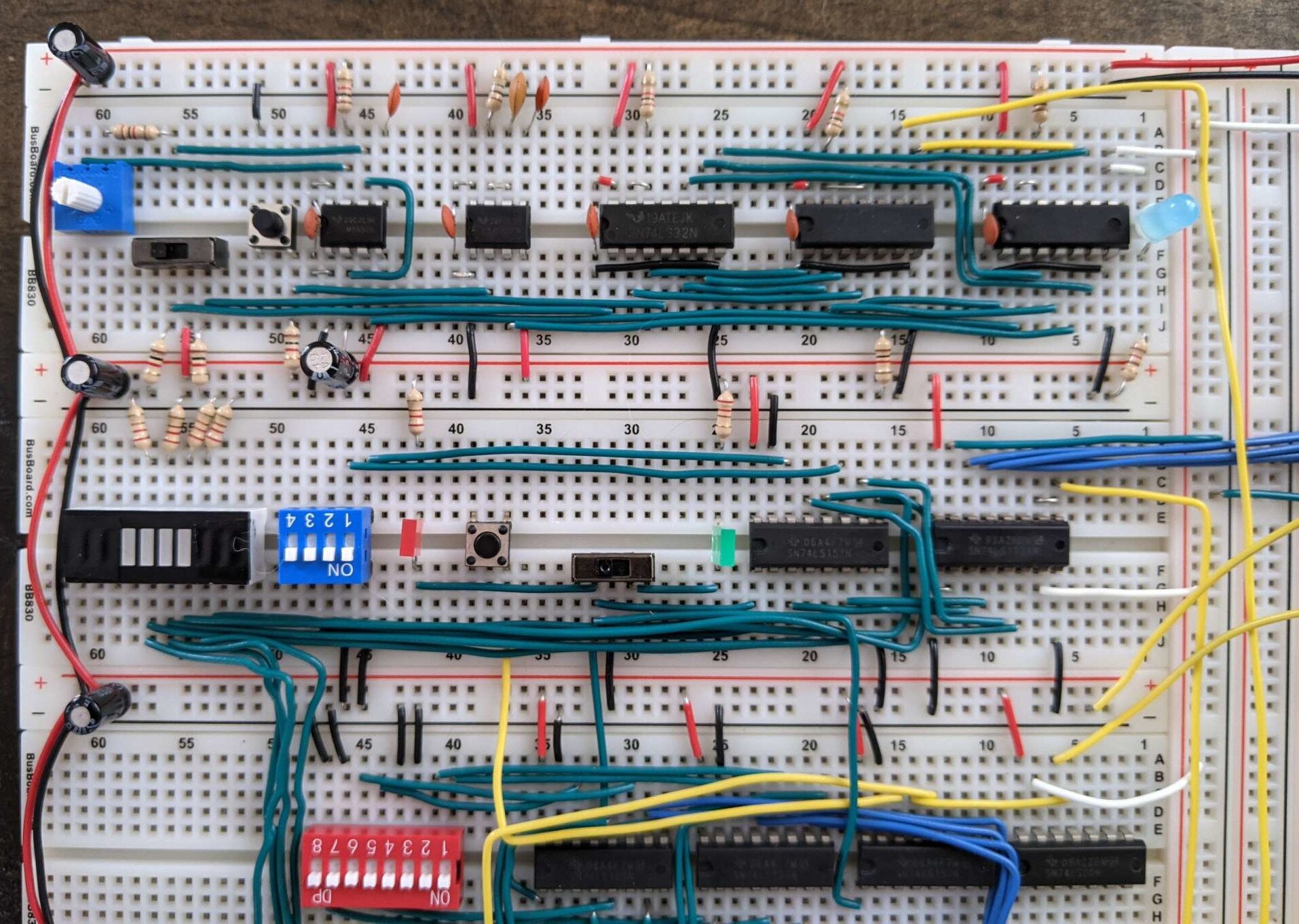
Central Power Rail
I still had the issue of bad power distribution through daisy chaining and it occurred to me that I could do with the power lines what I did with the clock and reset lines: run them down the middle.
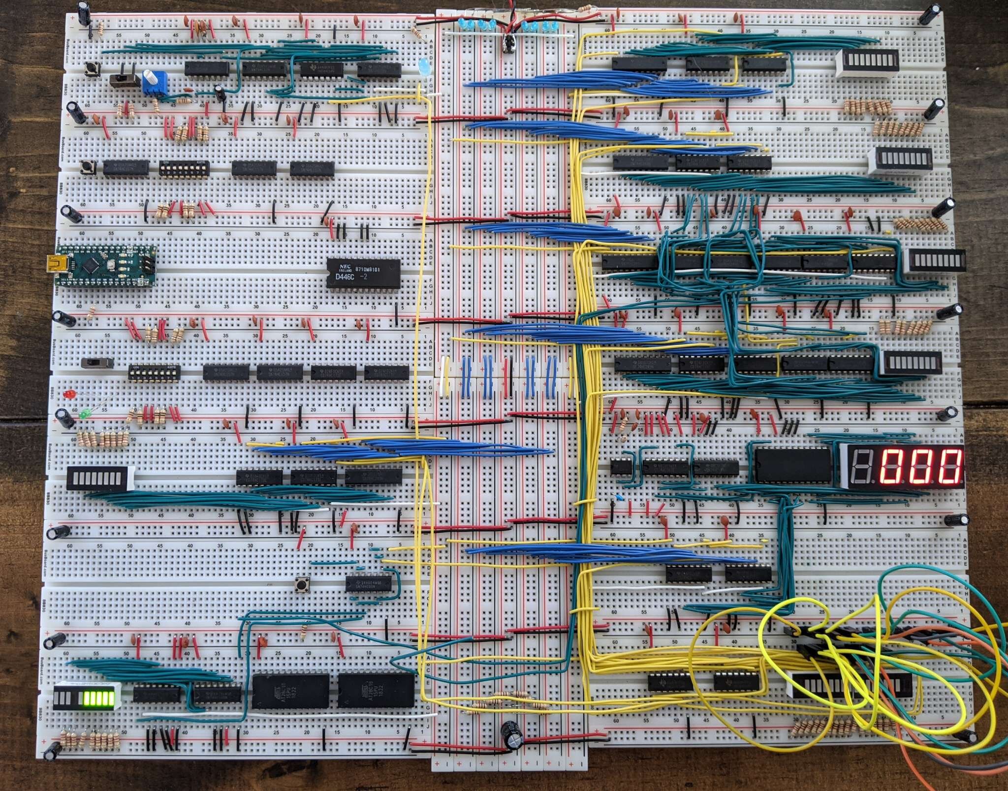
Better DIP Switches
The ones I had were hard to switch and kept popping out because they weren’t made for breadboards.
Relocate the Bypass Capacitors
I definitely wanted to have bypass capacitors but putting them physically next to the chips took up too much space. It was easier and near as good to put them next to the chip’s power wires instead.
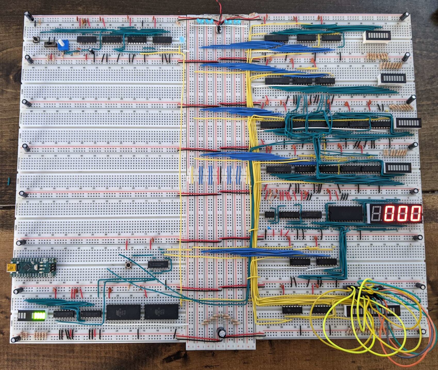
Wire Control Lines First
I realized that if I put down the yellow control wires first (and to a lesser extent the reset and clock wires), I could run the blue bus wires on top of them which would pin them down and limit their freedom to move around and cause problems.
Make Schematics Before Building
The process of hook things up for the first two builds was essentially looking at datasheets, making note of which pins connected to which pins, laying things out in my head, and then wiring it up. That led to mistakes as well as unclean wires because I didn’t have a big picture view.
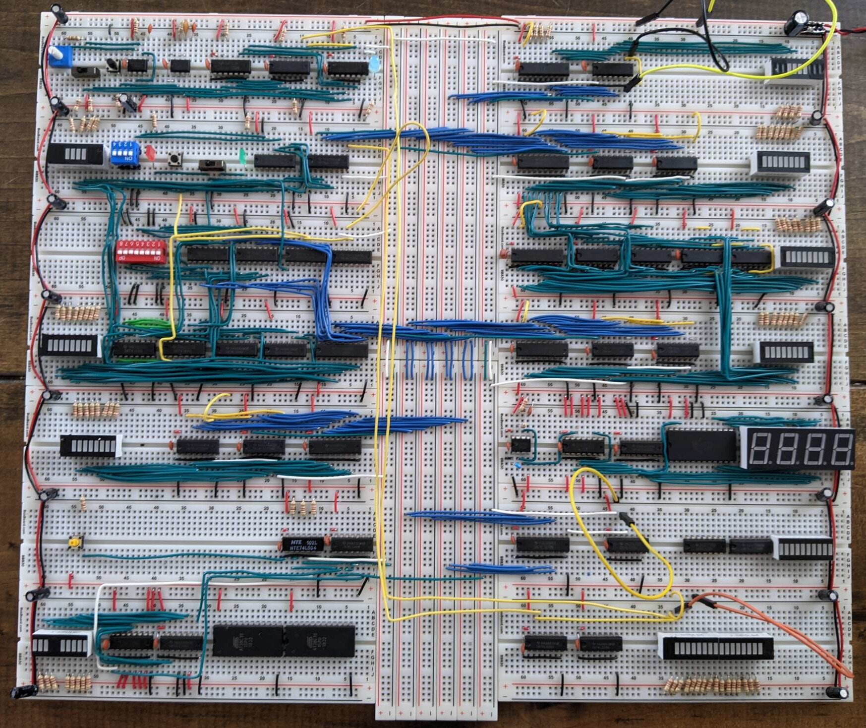
I started drawing schematics in KiCad first before hooking anything up which let me lay things out in a way that made better physical sense (e.g., trying to avoid crossing wires from the bottom of the boards to the top), and it was easier to reference a single schematic than multiple datasheets.
Complete and Test Each Module Fully
This one seems obvious but if you build everything in the order that Ben does, you’re often leaving modules incomplete until later. Having already built the thing twice before, I had a good idea of how everything worked as a whole so I could finish each module fully from top to bottom, right side first (except for the clock which is on the left side).
As an example, after the clock was finished I hooked up the Program Counter in its entirety: reset, clock, control, and bus. Ben leaves the control lines for when he discusses control logic and the bus lines for when he discusses the bus. I’m sure he did it that way for pedagogical purposes, but it makes for a bit of a mess having to go back and retrofit a module.
I set up the bus and the control LEDs immediately so that I could hook each module up fully before moving on.
556 Timer
Why use two chips when one will do?
256 Bytes of RAM
16 bytes of RAM seemed limiting.
Arduino Nano for Programming
I thought it would be nice to be able to program the thing with an Arduino instead of using the DIP switches all the time, but I never got around to doing it.
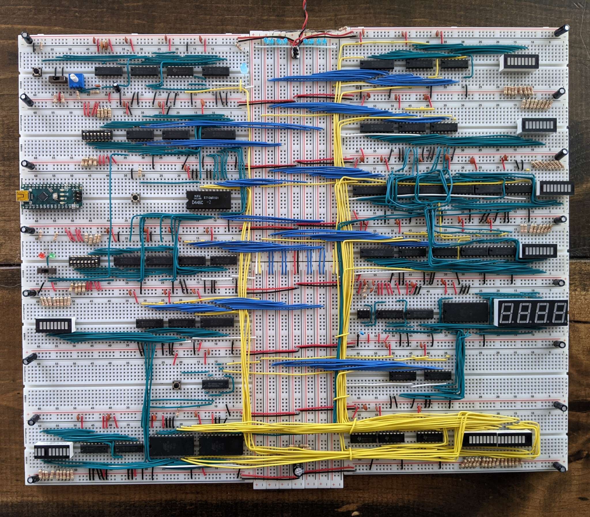
With that I began anew.
I wired from top to bottom, right side first, control signals always first. That ensured that all of the wires overlapped appropriately. (I’m still not happy with the ALU wiring but I got tired of bending wire.)
You can see the awesome DIP switches that not only look similar to the ICs, but they fit nice and snug into the breadboard.
And then I took a break for a month because I was on my third build and I was absolutely sick of cutting wire. But finally I mustered the energy to finish it, mostly because I kept having friends ask me what the hell I was building and I couldn’t really demonstrate anything interesting.
Conclusion
I loved this project and it was immensely satisfying to actually finish it. I had been following Ben’s work on YouTube for years but never started. Then I started and restarted and restarted again. And finally I finished it.
However, I realized near the end of the project that while I enjoyed the learning and the designing and the logic, the constant cutting and routing of wire was incredibly tedious. Small mistakes took a lot of work to fix and I was hesitant to try new things because of the effort involved. And this was on a breadboard where mistakes are easily fixed compared to doing rework on a printed circuit board.
Of the countless hours I spent on the project, I would guess that 90% of it was cutting wire, shaping wire, and debugging wire.
In fact, there’s a bug present in the above video. For some reason it only counts to 64 and then it restarts. And I don’t have any energy left to hunt down the issue. Maybe one day.
All of that is to say that I enjoy logic and hardware but the lack of flexibility is frustrating (coming from someone who writes software for a living). That has led me to start dabbling in FPGAs, and also recreating the computer on the Game Boy (more on that at a later date).
Last Edited: Dec 20, 2022