Building an FPGA Computer: SAP-1
I’ve been getting into FPGAs lately. Last year I built an FPGA version of Ben Eater’s breadboard computer, but I’ve been wanting to do a more advanced project to help me gain experience with Verilog and FPGAs in general.
For his breadboard computer, Ben Eater followed the design laid out in a book called Digital Computer Electronics by Malvino and Brown. The book builds what it calls the Simple-as-Possible (SAP) Computer. It starts with the incredibly simple SAP-1, adds some features to get the SAP-2, and then adds a few more to reach the final version called SAP-3.
Ben Eater’s version in the videos was mostly a SAP-1 with a few added instructions. I recreated his version essentially bit-for-bit in my FPGA implementation so it was also basically the SAP-1, but that was my first exposure to Verilog and FPGAs so my implementation was not the best: I had everything in one file instead of discrete modules, and I didn’t simulate anything to verify correctness.
I thought it might be a good experience to rebuild the SAP-1 using the Verilog skills I’ve learned since last year, but then also progressing to the SAP-2 and finishing with the SAP-3. I also thought it might be interesting to drive a display as well.
I made some minor changes to the version in the book where I thought it added clarity (e.g., making logic levels always active-high, giving signals more descriptive names, and removing the entire input/output system), but for the most part everything is the same as the book.
Overview
Modules
Every module has different behavior but most of them have a few signals in common: clk, rst, and out.
clk is a global signal which coordinates everything and ensure things happen when expected.
rst is a global signal that, when asserted, causes the computer to return to a known state, which in this case means resetting everything back to zero.
out is the output of each module which is then later connected to the bus for inter-module communication.
Clock
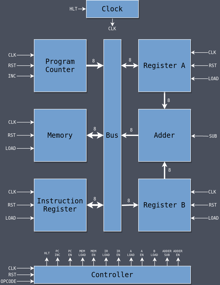
A computer can’t do anything without a clock. It’s the maestro that orchestrates all of the distinct components so that they can talk together at a fixed interval in lock-step with each other. A clock oscillates between HIGH and LOW repeatedly, until the end of time (or until power is removed). Without a clock there would be chaos. The clock is the beating heart of the computer.
I could have used the pre-defined CLK pin that is connected to the FPGA’s internal 16MHz clock, but instead I created a discrete clock module in its own Verilog file so I could control it with signals.
It has an input called clk_in and an output called clk_out. The output is always a copy of the input unless hlt is asserted in which case the output is just zero. That’s used later as part of the HLT instruction to stop computer execution.
If a program doesn’t need to be executed indefinitely then the final instruction can be HLT to stop all further execution. The easiest way to stop a computer from doing something is to stop its clock.
| |
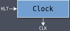
Program Counter
If you think of the clock as the maestro keeping the orchestra in time, and the orchestra as all of the individual components of the computer, then the Program Counter (PC) is the page of the music that everyone is playing. It always stores the address of the next instruction to be executed.
For the SAP-1, a program is just a series of bytes in memory where one byte makes up one instruction to be executed. The instructions are laid out serially and counted through starting from address 0. The SAP-1’s memory is only 16 bytes so the program counter should count from 0x0 (0) to 0xF (15).
If the clock goes high and inc is asserted, the value in the PC is incremented by one, otherwise it stays the same. Its value is always driven onto the output out so that it can be used outside of the module when necessary. A rst signal sets it back to zero.
| |
Register A

What good is a computer if it can’t store anything?
Registers are a computer’s way of storing data. Their size is normally dependent on the architecture of the computer: an 8-bit computer will have 8-bit registers, a 32-bit computer will have 32-bit registers, a 64-bit computer will have 64-bit registers, and so on. The computer is 8-bit so its registers are 8-bit as well.
Register A is the main register of the computer and many of the instructions depend upon it. Its internals look similar to some of the things seen previously: a clk, a rst, and an out.
bus is an input which is driven by some other module and Register A can read from it when it needs to load which happens when load is asserted.
| |
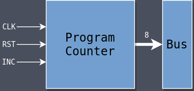
Register B
Register B is identical to Register A in design but when it’s used (as seen later), it never drives the bus directly; its output is fed to the Adder only. The SAP-1 is designed so that Register A is where the main action occurs and Register B supports it.
| |
Adder
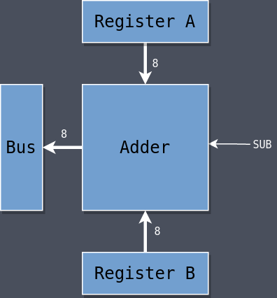
Computers were originally designed to help us do a lot of math very quickly so it makes sense that this humble computer should be able to do math also. The SAP-1 can only do addition and subtraction.
The two registers (A and B) are where all of the math operations occur: A + B or A - B. The arithmetic module is called the Adder even though it also does subtraction (subtraction is just addition of a negative number after all).
Notice the lack of a clock signal. The adder is constantly calculating either addition or subtraction based on the values in a and b and being placed directly onto its output out.
| |
Memory
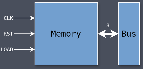
The SAP-1 has 16 bytes of memory which is small enough that it can be defined directly inside of the FPGA. With larger amounts of memory (possibly kilobytes or megabytes), it would be better to use an actual RAM chip as an external memory module.
There is a 4-bit register called the Memory Address Register (MAR) which is used to store a memory address. The SAP-1 takes two clock cycles to read from memory: one cycle loads an address from the bus into the MAR (using the load signal) and the second cycle uses the value in the MAR to address into ram and output that value onto the bus.
The initial block is used to initialize the memory by loading its contents from a file which is an easy way to set the memory. The file has sixteen lines where each line represents a byte of memory.
| |
Instruction Register
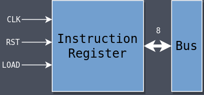
The program counter contains the memory address to read the next instruction from, and the memory itself contains the instructions at that address, but there also needs to be a way to actually get the instruction from memory.
Before an instruction can be interpreted and acted upon, it needs to be loaded from memory into a module that can separate the opcode from the data. That’s the job of the Instruction Register (IR).
An instruction has two components: the upper four bits are the opcode and the lower four bits are the operand. Some instructions use an operand and some don’t in which case it will be ignored.
The rst and load signals do what they’ve done in other modules and the entire instruction is driven onto the output out. Later on when its used its divided into its two 4-bit components: the opcode and operand.
| |
Bus
The bus is how all of the modules send data between themselves. When one module needs to send data to another, it puts it on the bus. When one module needs to receive data from another, it reads it from the bus. All is coordinated by certain signals being asserted at certain times: a load signal reads from the bus and an enable signal outputs onto the bus.
The bus is eight bits and nothing more than wires that go between every component in the computer. It’s eight bits wide because it’s an 8-bit computer. All data operations occur in units of eight bits.
In the original breadboard build, every module was connected directly to the bus through a logic chip that had an enable pin. The output of the module would flow through the chip unimpeded and drive the bus when the chip’s enable pin was asserted. The output of the module wouldn’t flow through the chip when the enable pin was not asserted, instead existing in a state of high impedance (high-Z). That feature ensured that only one module was ever driving the bus at a time.
Unfortunately FPGAs don’t have the ability to do high-Z in their internal logic so I couldn’t do that here. Instead, as shown in the module descriptions above, every module has an output called out which is always being driven by whatever value/logic the module contains. The controller then asserts an enable signal for whichever module’s output is needed on the bus.
To select the proper module to be the only one driving the bus, I multiplexed the five module outputs (adder_out, a_out, ir_out, mem_out, pc_out) using the five enable signals (adder_en, a_en, ir_en, mem_en, pc_en) as the select. When no enable signals are asserted, the bus is driven with zero.
| |
Controller
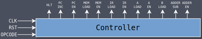
The controller is the most complicated part of the computer and is where all of the interesting stuff happens. It decides what the computer will do next by asserting the different control signals that have gone into each of the modules.
Those control signals are:
- hlt Halt execution of the computer
- pc_inc Increment the Program Counter
- pc_en Put the value in the Program Counter onto the bus
- mar_load Load an address into the Memory Address Register
- mem_en Put a value from memory onto the bus
- ir_load Load a value from the bus into the Instruction Register
- ir_en Put the value in the Instruction Register onto the bus
- a_load Load a value from the bus into A
- a_en Put the value in A onto the bus
- b_load Load a value from the bus into B
- adder_sub Subtract the value in B from A
- adder_en Put the adder’s value onto the bus
The controller module controls the behavior of the computer by asserting those signals at different times according to different stimuli.
Instruction execution occurs in a series of stages where each stage takes one clock cycle. The SAP-1 has six stages, starting at Stage 0 and counting to Stage 5, at which point it returns back to Stage 0 again. It continues on like that forever with every tick of the clock: 0, 1, 2, 3, 4, 5, 0, 1, 2, 3, 4, 5, etc.
There is a 3-bit stage register (allowing values from 0 to 7) and with each tick of the clock the stage increases by one. Once it hits 5, it goes back to 0. It changes stage on the negative clock edge so that the signals will be set up properly before the modules need them on the next positive clock edge.
opcode is passed from the IR into the controller module to do different things based on what instruction is currently executing. What it does depends on the instruction and the stage of execution.
Finally the output of the controller is the twelve control signals listed above. Different stages of different instructions will assert different signals to accomplish different things.
Rather than pass the signals in individually, I pass them all in a single 12-bit value where each bit represents one of the signals. That keeps the code cleaner and makes it easier to set all the bits to zero before setting the ones that need to be asserted at that time.
The SAP-1 has four operations that it can perform:
- [0000] LDA $X Load the value at memory location $X into A.
- [0001] ADD $X Add the value at memory location $X to A and store the sum in A.
- [0010] SUB $X Subtract the value at memory location $X from A and store the difference in A.
- [1111] HLT Halt execution of the program.
The values in the brackets represent the opcode and all but HLT have an operand. LDA, for example, has the opcode 0000 and its operand is the address of the value to be loaded into A.
Every instruction has the same first three stages which fetch the next instruction from memory based on the current value in the PC.
- All Instructions
- Stage 0
- Put the PC onto the bus (pc_en)
- Load that value into the MAR (mar_load)
- Stage 1
- Increment the PC (pc_inc)
- Stage 2
- Put whatever is in memory at the MAR address onto the bus (mem_en)
- Load it into the IR (ir_load)
- Stage 0
After the first three stages, the actions performed during the next three differ depending on the instruction, and some of the instructions do nothing at all.
- LDA
- Stage 3
- Put the instruction operand onto the bus (ir_en)
- Load that value into the MAR (mar_load)
- Stage 4
- Put whatever is in memory at the MAR address onto the bus (mem_en)
- Load that value into Register A (a_load)
- Stage 5
- Idle
- Stage 3
- ADD
- Stage 3
- Put the instruction operand onto the bus (ir_en)
- Load that value into the MAR (mar_load)
- Stage 4
- Put whatever is in memory at the MAR address onto the bus (mem_en)
- Load that value into Register B (b_load)
- Stage 5
- Put the value in the adder onto the bus (adder_en)
- Load that value into Register A (a_load)
- Stage 3
- SUB
- Stage 3
- Put the instruction operand onto the bus (ir_en)
- Load that value into the MAR (mar_load)
- Stage 4
- Put whatever is in memory at the MAR address onto the bus (mem_en)
- Load that value into Register B (b_load)
- Stage 5
- Do subtraction rather than addition (adder_sub)
- Put the value in the adder onto the bus (adder_en)
- Load that value into Register A (a_load)
- Stage 3
- HLT
- Stage 3
- Halt the clock (hlt)
- Stage 4
- Idle
- Stage 5
- Idle
- Stage 3
| |
Simulation
It’s always good to test a design in a testbench which allows for verifying correctness before uploading it to the FPGA. It’s much easier to catch and debug issues in simulation then it is once it’s on the actual FPGA.
| |
It instantiates all of the modules in the computer and connects them to each other. The initial block at the beginning runs once at the start of simulation to create a file called top_tb.vcd which contains all of the simulation data.
initial blocks aren’t synthesizable; they’re purely used for testing. In this case, one is used as a way of simulating a clock by toggling clk_in 128 times. With each iteration of the loop, clk_in is set to its inverse ~clk_in. So its state will be 0 -> 1 -> 0 -> 1 -> 0 -> 1, etc.
The #1 is a time delay, which again is non-synthesizable and used only for testing. The test waits one time unit, toggles the clock, loops, waits one time unit, toggles the clock, loops, 128 times.
So what’s the point? You can generate a simulation file and load it into a tool called gtkwave which will let you view the signals at different times.
After configuring it a bit to nicely show the signals that are important, it displays this:
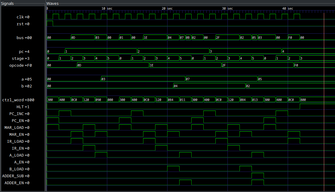
Here is the (annotated) test program:
$0 |   0D  // LDA [$D]   Load A with the value at address $D
$1 |   1E  // ADD [$E]   Add the value at address $E to A
$2 |   2F  // SUB [$F]   Subtract the value at address $F from A
$3 |   F0  // HLT        Stop execution
$4 |   00
$5 |   00
$6 |   00
$7 |   00
$8 |   00
$9 |   00
$A |   00
$B |   00
$C |   00
$D |   03  // Data: 3
$E |   04  // Data: 4
$F |   02  // Data: 2
Load the value at $D (3) into A, add to it the value in $E (4), subtract from it the value in $F (2), and then halt. At the end of execution the value in Register A should be 3+4-2=5. If you look at the location of the red marker, the clock is no longer ticking and the value in A is indeed 5.
It’s also useful (and neat) to trace the signals throughout time and see as each individual instruction executes: clock toggling, values going on and off the bus, register values changing, stages incrementing, control signals being asserted, etc.
Source Code
You can find all of the code here.
Last Edited: Feb 16, 2023