Building an FPGA Computer: SAP-2
Previously I built the SAP-1 on an FPGA based on a design laid out in the book Digital Computer Electronics by Malvino and Brown. Now it’s time to build the SAP-2, also from the book, which is quite a large step up from the SAP-1.
While the SAP-1 was explained in great detail in the book, the SAP-2 is much more vague and undefined. They don’t go into implementation details, provide schematics, or show the control signals. Instead they give a brief functional overview of its components, list out its instructions, and that’s about it. Thus I was forced to figure things out on my own, for better or for worse.
When creating my FPGA version, I decided to be content with it being functionally identical without getting hung up on the implementation details. As such, a program run on their theoretical version would have the same output as on mine, but the way it got there and the time it took to do it would be different.
This post is intended as a supplement to the first so I’ll assume readers of this one are familiar already with the SAP-1 to save me from repeating myself. I’ll refer back to it and mention ways that the SAP-2 differs.
The SAP-2 is akin to a teenager lying somewhere between the toddler SAP-1 and the adult SAP-3. While the SAP-1 and SAP-3 can stand on their own, the SAP-2 is trying to bridge the gap between them and does so quite poorly.
I didn't want to do the SAP-1 and then skip to the SAP-3, so my only choice was to recreate the behavior as written in the book, which made for some very awkward Verilog code.
Overview
Modules
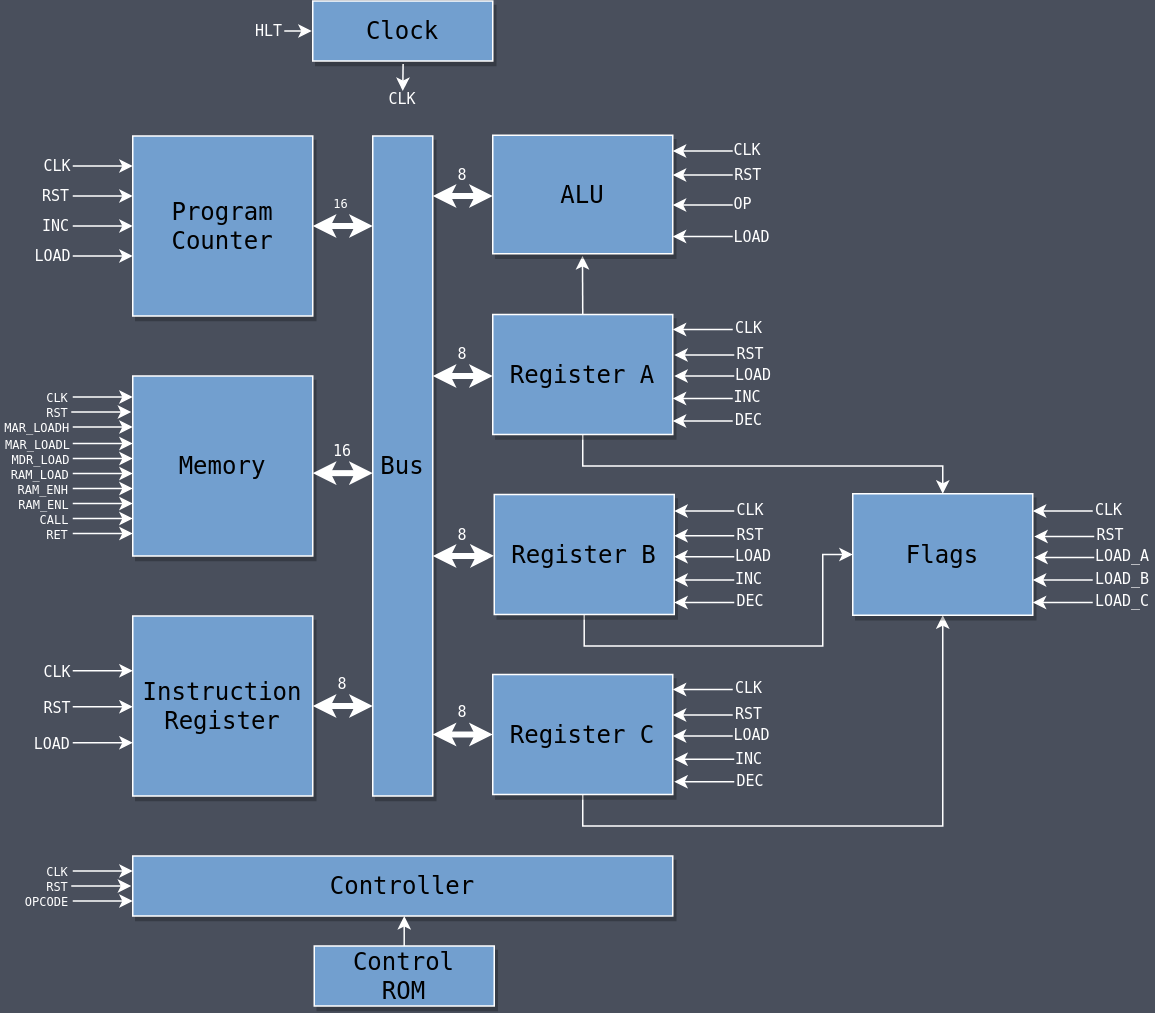
Clock
The clock is unchanged from the SAP-1.
| |
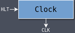
Program Counter
The program counter has been widened to 16 bits and it has an additional load signal.
The load signal loads the PC with a value taken from the bus, a requirement for being able to jump around during a program’s execution.
| |
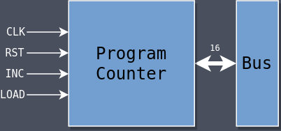
Registers A/B/C
There are now three registers: A, B, and C. Each are functionally identical so there is a single register module that is used for all three. It’s instantiated three times in the top module and given different names for each.
The book briefly mentions that register increments and decrements are done using the ALU, which would require putting a 1 into the ALU’s temp register, putting the contents of B or C into A, and then doing an addition or a subtraction. But it doesn’t explain where that 1 comes from, how to avoid the A register being overwritten for increments and decrements of B or C, or how it’s supposed to be done in only four T-states.
I instead opted to give each register an inc and a dec signal to increment and decrement, respectively, rather than go through the ALU. I may figure out a way to use the ALU directly when it comes time to build the SAP-3.
| |
ALU
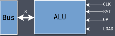
The Arithmetic Logic Unit (ALU) is the same as the SAP-1’s Adder but with the ability to do logic operations.
The temporary register has been moved inside of the ALU module itself which can be loaded with the load signal which frees up Register B for other uses. Register A continues to be the primary register for operations, using the temp register as the other operand when required. The control logic is responsible for filling the temp register with the necessary data prior to doing the operation.
The ALU can perform eight operations:
- Addition (ADD)
- Subtraction (SUB)
- Logical AND (AND)
- Logical OR (OR)
- Logical XOR (XOR)
- Complement (CMA)
- Rotate All Left (RAL)
- Rotate All Right (RAR)
An arithmetic shift left will move the bits that are shifted out the left side into the right side, while an arithmetic shift right will move zeroes into the left side.
The operation to be performed is determined by the op signal.
| |
Flags Register
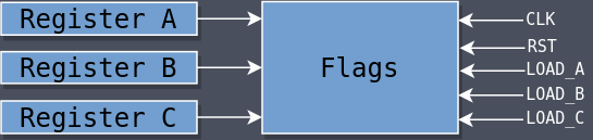
The flags register is a special register used to hold the status of previous operations. There are two:
- Zero Flag: Set if the previous operation caused a result of 0.
- Sign Flag: Set if the previous operation caused a negative result.
It’s a bit unusual that the flags register is connected to A/B/C directly instead of to the ALU, but that was required so that the INR and DCR instructions would update the flags without going through the ALU, as discussed above.
Not all instructions should update the flags so there are three signals that dictate whether or not the flags are updated based on the contents of each of the three registers: load_a, load_b, and load_c.
For example, INR C operates on Register C, so the control logic asserts load_c so that the flags are updated based on the contents of C. If the increment operation causes C to become zero then FLAG_Z is set. If the operation causes C to become negative then FLAG_S is set.
But the instruction MVI C, A, which copies the contents of A into C, should not update the flags, and so the load_c signal is not asserted during that instruction.
| |
Memory
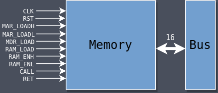
The memory has been expanded to 64K which requires a 16-bit address space to be able to address from 0x0000 to 0xFFFF. The expansion to 16-bit requires more complicated control logic which requires more control signals.
The Memory Address Register (MAR) holds memory address so it was expanded to 16-bit which required separate signals for loading the high byte (mar_loadh) and the low byte (mar_loadl).
There is also a new internal register called the Memory Data Register (MDR) which holds values temporarily when reading from or writing to the memory. mdr_load loads into the MDR from the bus and ram_load loads into memory from the MDR.
The MDR is 16-bit even though data values should only be 8-bit because certain instructions (namely LDA and STA) require holding two separate values in the MDR at one time. The high byte is loaded with ram_enh and the low byte is loaded with ram_enl. I’m not sure if this was what Malvino and Brown had in mind but it works.
The call signal loads two special memory locations (0xFFFE and 0xFFFF) with the contents of the bus and the ret signal loads from those two locations into the MDR to be later put back into the PC. These two signals are used to facilitate the CALL and RET instructions which will be discussed later. The implication of this rudimentary system is that a function cannot call another function or else the return address will be overwritten. The SAP-3 will fix that.
| |
Instruction Register
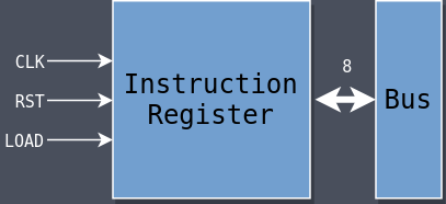
The Instruction Register (IR) is unchanged from the SAP-1 except that it only uses the lower eight bits of the bus during a load.
| |
Instructions
There are 39 instructions which is a lot more than the SAP-1. The book also includes an IN and an OUT but I removed those because they don’t make sense for the version I’m building.
The book uses the same opcodes for the instructions as the Intel 8080 and I did the same to stay consistent. The authors provide the number of T-states that are required for each instruction but I was unable to reach the same values for many of the instructions. In some cases my implementation uses fewer T-states and in some others it uses more.
In particular, the INR and DCR instructions don’t make sense as described by Malvino and Brown. They claim that those two instructions use Register A for those operations but if that were true then the contents of A would be lost and it would take a lot more than four T-states as they claim. I decided to use explicit inc and dec signals for each of the three main registers to allow for directly incrementing and decrementing them in a single T-state.
Some instructions update the flags and some do not. If an instruction operates on a particular register then the flags are updated based on the conditions of that register (e.g., INR B will update the flags if B becomes 0 or negative).
There are four Address Modes:
- Direct
- Required data is located at memory address which follows the opcode
- Immediate
- Required data is specified in the instruction itself
- Register
- Required data is inside of a register
- Implied
- Required data is implied by the opcode
Every instruction takes at least three T-states because it takes three just to fetch the instruction from memory. The instructions with the most T-states are those that deal deal with memory addresses because of the time required to shuffle addresses from the PC to the MAR and MDR.
JM, JNZ, and JZ take a variable number of cycles depending on whether the jump occurs or not. If the jump occurs it takes eight T-states, otherwise it takes four.
The length of my instructions differ from those in the book and are faster in many places, but not all. I tried to think of solutions that would match theirs exactly but was unable to figure out how they get their numbers.
| Instruction | Opcode | T States | Flags | Addressing | Bytes | Description |
|---|---|---|---|---|---|---|
| ADD B | 80 | 5 | S,Z | Register | 1 | A = A + B |
| ADD C | 81 | 5 | S,Z | Register | 1 | A = A + C |
| ANA B | A0 | 5 | S,Z | Register | 1 | A = A & B |
| ANA C | A1 | 5 | S,Z | Register | 1 | A = A & C |
| ANI byte | E6 | 7 | S,Z | Immediate | 2 | A = A & byte |
| CALL addr | CD | 9 | - | Immediate | 3 | Call function at addr |
| CMA | 2F | 4 | - | Implied | 1 | A = ~A |
| DCR A | 3D | 4 | S,Z | Register | 1 | A = A - 1 |
| DCR B | 05 | 4 | S,Z | Register | 1 | B = B - 1 |
| DCR C | 0D | 4 | S,Z | Register | 1 | C = C - 1 |
| HLT | 76 | 4 | - | - | 1 | Halt execution |
| INR A | 3C | 4 | S,Z | Register | 1 | A = A + 1 |
| INR B | 04 | 4 | S,Z | Register | 1 | B = B + 1 |
| INR C | 0C | 4 | S,Z | Register | 1 | C = C + 1 |
| JMP addr | C3 | 8 | - | Immediate | 3 | Jump to addr |
| JM addr | FA | 4/8 | - | Immediate | 3 | Jump to addr if S Flag == 1 |
| JNZ addr | C2 | 4/8 | - | Immediate | 3 | Jump to addr if Z Flag == 0 |
| JZ addr | CA | 4/8 | - | Immediate | 3 | Jump to addr if Z flag == 1 |
| LDA addr | 3A | 10 | - | Direct | 3 | Load A with value at addr |
| MOV A, B | 78 | 4 | - | Register | 1 | A = B |
| MOV A, C | 79 | 4 | - | Register | 1 | A = C |
| MOV B, A | 47 | 4 | - | Register | 1 | B = A |
| MOV B, C | 41 | 4 | - | Register | 1 | B = C |
| MOV C, A | 4F | 4 | - | Register | 1 | C = A |
| MOV C, B | 48 | 4 | - | Register | 1 | C = B |
| MVI A, byte | 3E | 6 | - | Immediate | 2 | A = byte |
| MVI B, byte | 06 | 6 | - | Immediate | 2 | B = byte |
| MVI C, byte | 0E | 6 | - | Immediate | 2 | C = byte |
| NOP | 00 | 3 | - | - | 1 | Do nothing |
| ORA B | B0 | 5 | S,Z | Register | 1 | A = A |
| ORA C | B1 | 5 | S,Z | Register | 1 | A = A |
| ORI byte | F6 | 7 | S,Z | Immediate | 2 | A = A |
| RAL | 17 | 4 | - | Implied | 1 | A « 1, LSB becomes zero |
| RAR | 1F | 4 | - | Implied | 1 | A » 1, MSB goes to LSB |
| RET | C9 | 5 | - | Implied | 1 | Return from function |
| STA addr | 32 | 9 | - | Direct | 3 | Store value in A at addr |
| SUB B | 90 | 5 | S,Z | Register | 1 | A = A - B |
| SUB C | 91 | 5 | S,Z | Register | 1 | A = A - C |
| XRA B | A8 | 5 | S,Z | Register | 1 | A = A ^ B |
| XRA C | A9 | 5 | S,Z | Register | 1 | A = A ^ C |
| XRI byte | EE | 7 | S,Z | Immediate | 2 | A = A ^ byte |
Bus
The bus has been widened to 16 bits to accommodate the memory address space and, like the SAP-1, a multiplexor is used to select which module gets to output onto the bus at any one time.
| |
Controller
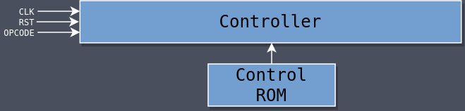
The SAP-2 has 35 control signals (23 more than the SAP-1) and the longest instruction takes 10 T-states (four more than the longest SAP-1 instruction). Trying to implement all of that logic with a switch statement like we did for the SAP-1 would result in a massive module that would be hard to write, hard to understand, and hard to debug.
Fortunately control logic is combinational logic, and all combinational logic can be represented in the form of Read-Only Memory (ROM) by using the inputs to the combinational logic to address into the ROM. The value stored at that address is the output corresponding to those inputs.
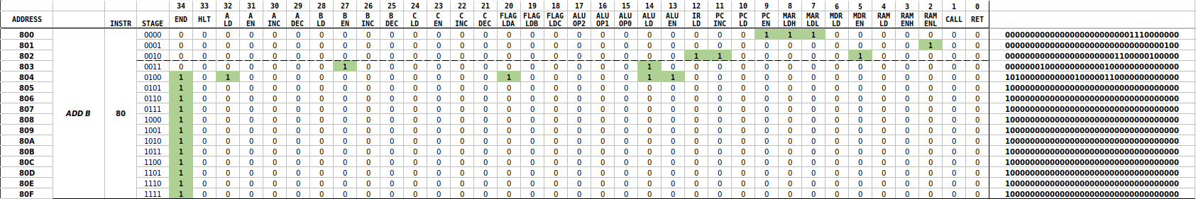
Every instruction is one byte (eight bits) and the maximum required number of T-states is 10 (requiring four bits to represent). We can combine those together into a single 12-bit address. The instruction goes into bits 11-4 and the T-state value goes into bits 3-0: IIIIIIII TTTT. Then, if we want to know what control signal should be asserted for a given instruction and certain T-state, we can look it up in the ROM.
For example, if the instruction is ADD B ($80) and we’re on stage 3, we concatenate $80 and $3 together to get address $803. The value at that address is the 35-bit control word detailing which signals to assert at that point in time. In this case: 00000001000000000000100000000000000, where the two asserted signals are B_EN and ALU_LOAD.
The question is: how to fill out the ROM? A 12-bit address means 4096 different values to program which would be a major pain (and error-prone) to do by hand. Instead I used a spreadsheet where the rows are the addresses and the columns are the different control signals and used the CONCATENATE() function to concatenate all of the signal bits into a single string. Then it was just a matter of copying that entire binary string column into a file which could be loaded in Verilog using readmemb.
A lot of space is wasted because because the 12-bit address allows for 256 instructions but there are only 41. If the SAP-2 wasn’t using a subset of the Intel 8080 instruction set then the instruction op codes could start at $00 and go up to $25, reducing the number of address lines required to six. But using the 8080 instruction set means we can use existing 8080 programs which is useful.
Given that the control ROM contains all of the logic, the actual controller itself doesn’t do much anymore. Mostly it just handles the special logic required for the jump instructions, where it checks the flag states if the current instruction is JZ, JNZ, or JM, and if it’s currently in stage 4, which is where a decision needs to be made.
Other than that, it increments the stage like usual, and pulls the current control word out of the ROM based on the current instruction and stage acting as the address.
There is also a special signal called END which is used to reset the stage back to 0 when an instruction has finished so that all 16 possible T-states don’t have to cycle through before the next instruction begins. Every instruction ends with that signal asserted, as shown in the spreadsheet image above.
| |
Programming
The SAP-2 uses a subset of the Intel 8080 instruction set which has the nice benefit of being able to use existing 8080 tools for our version, like an assembler. The Pretty 8080 Assembler lets you write 8080 assembly and then assembles it into various forms for you.
Here’s a perfectly valid 8080 program written in assembly using only the subset of instructions listed above:
| |
Here it is annotated with addresses, opcodes, and operands:
| |
Using the HEX button in the assembler will write out the program as hex values to a file on disk, but unfortunately it also includes extra characters we don’t want. Instead we can use the BIN button to write out actual binary data instead. Then we can use a tool called hexdump to convert that to hex for us which we can then read into memory inside of Verilog.
| |
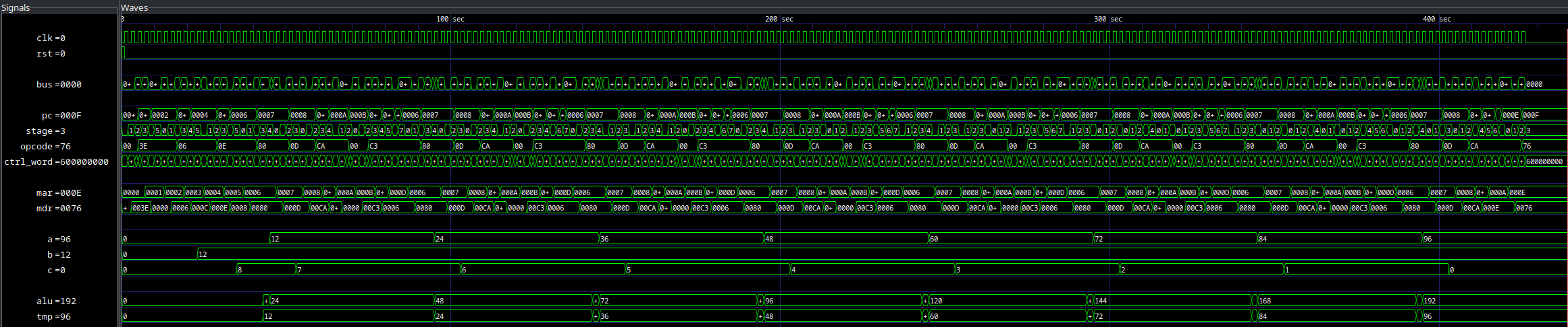
Simulation
Again we use a testbench to simulate the design and verify correctness.
| |
Simulation generates the following waveforms, where the final value of A is 96 as expected:
Source Code
You can find all of the code here.
Last Edited: Feb 27, 2023