Previously I built the SAP-1 and SAP-2 in Verilog based on a design laid out in the book Digital Computer
Electronics by Malvino and
Brown. Now it’s time to build the final evolution of the computer from that book, the SAP-3.
The SAP-1 was very simplistic but very well-explained. The SAP-2 was a big step up from the SAP-1
but explained rather poorly, and it required me to do a lot of awkward things with its design to get
it to match the spec laid out in the book. The SAP-3 is even more complex than the SAP-2 but
thankfully it didn’t require an awkward design because it’s essentially an Intel 8080/8085 with some
instructions removed.
Once again when creating my FPGA version, I decided to be content with it being functionally
identical without getting hung up on the implementation details. A program written for the SAP-3
should have the same output when run on my version, but it may finish in more or less time.
This post is intended as a supplement to the first and second so I’ll assume readers of this one are familiar
already with the SAP-1 and SAP-2.
Overview
The SAP-3 supports more instructions, has more registers, and has a more complicated ALU, but
it’s actually more simple than the SAP-2 because of the design of the instructions and how they
encode various data (to be explained later).
If you compare this overview architecture diagram to the SAP-2 it looks much simpler with fewer
control signals even though it’s a more capable machine.
The SAP-1 and SAP-2 had discrete register modules while the SAP-3 has a single module called the
Register File which contains all of the other registers.
There are six 8-bit programmer-accessible registers available: B, C, D, E, H,
and L.
The 8-bit registers can be paired together for some instructions to form three 16-bit registers:
BC, DE, and HL.
There are also two dedicated 16-bit registers with special functions: the Program Counter (PC)
and the Stack Pointer (SP). They’re always operated on as 16-bits but they’re laid out in
Verilog as two 8-bit values.
The PC in the SAP-1 and SAP-2 was its own module but now it’s been brought into the register file.
The SAP-2 had a stack but it was hard-coded to be the two bytes at addresses 0xFFFE and 0xFFFF. The
SAP-3 uses SP to point to the address of the bottom of the stack.
There are also two 8-bit programmer-inaccessible registers: W and Z. They’re used as
temporary storage for certain instructions. The SAP-2 was missing them which ended up
overcomplicating the memory module as it was responsible for holding temporary data in its Memory
Data Register.
The registers are laid out in the array called data in a specific order:
0000 - B
0001 - C
0010 - D
0011 - E
0100 - H
0101 - L
0110 - W
0111 - Z
1000 - P
1001 - C
1010 - S
1011 - P
I chose that order because, as shown later, all of the instructions encode the registers in that
order as well (at least for B-L). That makes it simple to take the bits from the opcode and pass
them in directly through the rd_sel and wr_sel inputs. When needing to referencing W, Z, PC,
or SP, they’re explicitly enabled.
16-bit increments and decrements (instructions INX and DCX) go through the register file
rather than the ALU because they shouldn’t affect the flags. Whether to perform an increment or
decrement comes from the ext signal. There is also the ability to do a double increment which is
used for skipping over the address bytes of a conditional jump when the condition is not met.
rd_sel and wr_sel are five bits even though only four are needed to encode the twelve
registers; bit 5 is set when the register should be treated as the 16-bit extended register. For
example, if rd_sel is 10000, then BC should be read.
The ALU has been expanded significantly from the SAP-2 to support more operations. It has the
standard 8-bit accumulator (acc) which is used for all of its operations as well as two
temporary registers: act and tmp. When an operation requires two operands, one is acc
and the other is tmp. When an operation needs to use the accumulator but doesn’t want to
overwrite its value, acc is copied to act and then act is later copied to acc.
The flags register from the SAP-2 has been moved inside of the ALU which is how it is normally done.
There are four flags: Zero (Z), Carry (C), Parity (P), and Sign (S). The flags are
set differently depending on the operation as some operations should not affect certain flags.
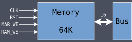
The memory module is significantly less complicated this time around. It has the 64K of memory in
ram and then a 16-bit Memory Address Register (MAR) to hold addresses that it can then use
for reading and writing from memory. No other logic is needed.
The bus is similar to how it was in SAP-1 and SAP-2 but with different signals. This time there are
only four output signals which ever drive the bus: reg_oe, mem_oe, alu_oe, and
alu_flags_oe.
The controller for the SAP-1 used a case statement to assert the different control signals depending
on the opcode and the current stage of execution. That was possible because there were so few
instructions.
The controller for the SAP-2 instead used a control ROM to hold the different signals because it had
more instructions and a lot of Verilog would have needed to be written to manage all of the
different instructions.
For the SAP-3, I’ve gone back to the case statement approach because, even though there are many
more instructions than the SAP-2, they’ve been decoded such that we can
extract the relevant bits from the opcode and control the signals in a way that is logical and makes
sense.
It still makes for quite a lot of Verilog (nearly 1000 lines) but it’s all much more readable and
understandable than trying to fill out a spreadsheet like was done for the SAP-2. It is also likely
more inline with how instructions were decoded for the actual Intel 8080/8085.
Rather than listing all of the code here, I’ll talk about it in the dedicated Instruction
Decoding section.
Instruction Set
The SAP-3 has the same instruction set as the Intel 8085 but with some instructions left out. I’ve
listed all of the instructions I implemented in the following table, leaving out those not mentioned
in the book, while also removing IN and OUT as they aren’t really relevant here. They’ve been
ordered by similarity of function rather than alphabetically or by opcode.
The T states shown in the table are the number of cycles required to complete the entire instruction
as implemented in my version, which are sometimes higher than the actual 8085 and sometimes lower.
The 8085 has eight flags but the SAP-3 only has four:
[S]ign - the instruction resulted in a value less than zero
[Z]ero - the instruction resulted in a value of zero
[P]arity - the instruction resulted in even (0) or odd (1) parity
[C]arry - the instruction resulted in a carry bit
Descriptive Table
Instruction
Opcode
Bytes
Flags
T States
Description
INR A
3C
1
SZP-
4
A = A + 1
INR B
04
1
SZP-
6
B = B + 1
INR C
0C
1
SZP-
6
C = C + 1
INR D
14
1
SZP-
6
D = D + 1
INR E
1C
1
SZP-
6
E = E + 1
INR H
24
1
SZP-
6
H = H + 1
INR L
2C
1
SZP-
6
L = L + 1
INR M
34
1
SZP-
7
[HL] = [HL] + 1
DCR A
3D
1
SZP-
4
A = A - 1
DCR B
05
1
SZP-
6
B = B - 1
DCR C
0D
1
SZP-
6
C = C - 1
DCR D
15
1
SZP-
6
D = D - 1
DCR E
1D
1
SZP-
6
E = E - 1
DCR H
25
1
SZP-
6
H = H - 1
DCR L
2D
1
SZP-
6
L = L - 1
DCR M
35
1
SZP-
7
[HL] = [HL] - 1
INX B
03
1
----
4
BC = BC + 1
INX D
13
1
----
4
DE = DE + 1
INX H
23
1
----
4
HL = HL + 1
INX SP
33
1
----
4
SP = SP + 1
DCX B
0B
1
----
4
BC = BC - 1
DCX D
1B
1
----
4
DE = DE - 1
DCX H
2B
1
----
4
HL = HL - 1
DCX SP
3B
1
----
4
SP = SP - 1
DAD B
09
1
---C
12
HL = HL + BC
DAD D
19
1
---C
12
HL = HL + DE
DAD H
29
1
---C
12
HL = HL + HL
DAD SP
39
1
---C
12
HL = HL + SP
ADD A
87
1
SZPC
4
A = A + A
ADD B
80
1
SZPC
5
A = A + B
ADD C
81
1
SZPC
5
A = A + C
ADD D
82
1
SZPC
5
A = A + D
ADD E
83
1
SZPC
5
A = A + E
ADD H
84
1
SZPC
5
A = A + H
ADD L
85
1
SZPC
5
A = A + L
ADD M
86
1
SZPC
6
A = A + [HL]
ADI byte
C6
2
SZPC
6
A = A + byte
ADC A
8F
1
SZPC
4
A = A + A + FlagC
ADC B
88
1
SZPC
5
A = A + B + FlagC
ADC C
89
1
SZPC
5
A = A + C + FlagC
ADC D
8A
1
SZPC
5
A = A + D + FlagC
ADC E
8B
1
SZPC
5
A = A + E + FlagC
ADC H
8C
1
SZPC
5
A = A + H + FlagC
ADC L
8D
1
SZPC
5
A = A + L + FlagC
ADC M
8E
1
SZPC
6
A = A + [HL] + FlagC
ACI byte
CE
2
SZPC
6
A = A + byte + FlagC
SUB A
97
1
SZPC
4
A = A - A
SUB B
90
1
SZPC
5
A = A - B
SUB C
91
1
SZPC
5
A = A - C
SUB D
92
1
SZPC
5
A = A - D
SUB E
93
1
SZPC
5
A = A - E
SUB H
94
1
SZPC
5
A = A - H
SUB L
95
1
SZPC
5
A = A - L
SUB M
96
1
SZPC
6
A = A - [HL]
SUI byte
D6
2
SZPC
6
A = A - byte
SBB A
9F
1
SZPC
4
A = A - byte - FlagC
SBB B
98
1
SZPC
5
A = A - byte - FlagC
SBB C
99
1
SZPC
5
A = A - byte - FlagC
SBB D
9A
1
SZPC
5
A = A - byte - FlagC
SBB E
9B
1
SZPC
5
A = A - byte - FlagC
SBB H
9C
1
SZPC
5
A = A - byte - FlagC
SBB L
9D
1
SZPC
5
A = A - byte - FlagC
SBB M
9E
1
SZPC
6
A = A - byte - FlagC
SBI byte
DE
2
SZPC
6
A = A - byte - FlagC
ANA A
A7
1
SZPC
4
A = A and A
ANA B
A0
1
SZPC
5
A = A and B
ANA C
A1
1
SZPC
5
A = A and C
ANA D
A2
1
SZPC
5
A = A and D
ANA E
A3
1
SZPC
5
A = A and E
ANA H
A4
1
SZPC
5
A = A and H
ANA L
A5
1
SZPC
5
A = A and L
ANA M
A6
1
SZPC
6
A = A and [HL]
ANI byte
E6
2
SZPC
6
A = A and byte
ORA A
B7
1
SZPC
4
A = A or A
ORA B
B0
1
SZPC
5
A = A or B
ORA C
B1
1
SZPC
5
A = A or C
ORA D
B2
1
SZPC
5
A = A or D
ORA E
B3
1
SZPC
5
A = A or E
ORA H
B4
1
SZPC
5
A = A or H
ORA L
B5
1
SZPC
5
A = A or L
ORA M
B6
1
SZPC
6
A = A or [HL]
ORI byte
F6
2
SZPC
6
A = A or byte
XRA A
AF
1
SZPC
4
A = A xor A
XRA B
A8
1
SZPC
5
A = A xor B
XRA C
A9
1
SZPC
5
A = A xor C
XRA D
AA
1
SZPC
5
A = A xor D
XRA E
AB
1
SZPC
5
A = A xor E
XRA H
AC
1
SZPC
5
A = A xor H
XRA L
AD
1
SZPC
5
A = A xor L
XRA M
AE
1
SZPC
6
A = A xor [HL]
XRI byte
EE
2
SZPC
6
A = A xor byte
RLC
07
1
---C
4
Shift A left and FlagC = A[7]
RAL
17
1
---C
4
Shift A left and shift FlagC into A[0]
RAR
1F
1
---C
4
Shift A right and shift FlagC into A[7]
RRC
0F
1
---C
4
Shift A right and FlagC = A[0]
CMA
2F
1
----
4
A = ~A
STC
37
1
---C
4
FlagC = 1
CMC
3F
1
---C
4
FlagC = ~FlagC
CMP A
BF
1
SZPC
4
FlagZ = 1 if A == A
CMP B
B8
1
SZPC
5
FlagZ = 1 if A == B
CMP C
B9
1
SZPC
5
FlagZ = 1 if A == C
CMP D
BA
1
SZPC
5
FlagZ = 1 if A == D
CMP E
BB
1
SZPC
5
FlagZ = 1 if A == E
CMP H
BC
1
SZPC
5
FlagZ = 1 if A == H
CMP L
BD
1
SZPC
5
FlagZ = 1 if A == L
CMP M
BE
1
SZPC
6
FlagZ = 1 if A == [HL]
CPI byte
FE
2
----
6
FlagZ = 1 if A == byte
LDA addr
3A
3
----
11
Load A with [addr]
LDAX B
0A
1
----
8
Load A with [BC]
LDAX D
1A
1
----
8
Load A with [DE]
LXI B, dble
01
3
----
10
Load BC with dble
LXI D, dble
11
3
----
10
Load DE with dble
LXI H, dble
21
3
----
10
Load HL with dble
LXI SP, dble
31
3
----
10
Load SP with dble
STA addr
32
3
----
11
Store A at [addr]
STAX B
02
1
----
8
Store A at [BC]
STAX D
12
1
----
8
Store A at [DE]
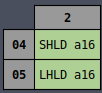
LHLD addr
2A
3
----
14
Load HL with [addr]
SHLD addr
22
3
----
14
Store HL at [addr]
MOV A, A
7F
1
----
4
A = A
MOV A, B
78
1
----
4
A = B
MOV A, C
79
1
----
4
A = C
MOV A, D
7A
1
----
4
A = D
MOV A, E
7B
1
----
4
A = E
MOV A, H
7C
1
----
4
A = H
MOV A, L
7D
1
----
4
A = L
MOV A, M
7E
1
----
5
A = [HL]
MOV B, A
47
1
----
4
B = A
MOV B, B
40
1
----
4
B = B
MOV B, C
41
1
----
4
B = C
MOV B, D
42
1
----
4
B = D
MOV B, E
43
1
----
4
B = E
MOV B, H
44
1
----
4
B = H
MOV B, L
45
1
----
4
B = L
MOV B, M
46
1
----
5
B = [HL]
MOV C, A
4F
1
----
4
C = A
MOV C, B
48
1
----
4
C = B
MOV C, C
49
1
----
4
C = C
MOV C, D
4A
1
----
4
C = D
MOV C, E
4B
1
----
4
C = E
MOV C, H
4C
1
----
4
C = H
MOV C, L
4D
1
----
4
C = L
MOV C, M
4E
1
----
5
C = [HL]
MOV D, A
57
1
----
4
D = A
MOV D, B
50
1
----
4
D = B
MOV D, C
51
1
----
4
D = C
MOV D, D
52
1
----
4
D = D
MOV D, E
53
1
----
4
D = E
MOV D, H
54
1
----
4
D = H
MOV D, L
55
1
----
4
D = L
MOV D, M
56
1
----
5
D = [HL]
MOV E, A
5F
1
----
4
E = A
MOV E, B
58
1
----
4
E = B
MOV E, C
59
1
----
4
E = C
MOV E, D
5A
1
----
4
E = D
MOV E, E
5B
1
----
4
E = E
MOV E, H
5C
1
----
4
E = H
MOV E, L
5D
1
----
4
E = L
MOV E, M
5E
1
----
5
E = [HL]
MOV H, A
67
1
----
4
H = A
MOV H, B
60
1
----
4
H = B
MOV H, C
61
1
----
4
H = C
MOV H, D
62
1
----
4
H = D
MOV H, E
63
1
----
4
H = E
MOV H, H
64
1
----
4
H = H
MOV H, L
65
1
----
4
H = L
MOV H, M
66
1
----
5
H = [HL]
MOV L, A
6F
1
----
4
L = A
MOV L, B
68
1
----
4
L = B
MOV L, C
69
1
----
4
L = C
MOV L, D
6A
1
----
4
L = D
MOV L, E
6B
1
----
4
L = E
MOV L, H
6C
1
----
4
L = H
MOV L, L
6D
1
----
4
L = L
MOV L, M
6E
1
----
5
L = [HL]
MOV M, A
77
1
----
5
[HL] = A
MOV M, B
70
1
----
5
[HL] = B
MOV M, C
71
1
----
5
[HL] = C
MOV M, D
72
1
----
5
[HL] = D
MOV M, E
73
1
----
5
[HL] = E
MOV M, H
74
1
----
5
[HL] = H
MOV M, L
75
1
----
5
[HL] = L
MVI A, byte
3E
2
----
6
A = byte
MVI B, byte
06
2
----
6
B = byte
MVI C, byte
0E
2
----
6
C = byte
MVI D, byte
16
2
----
6
D = byte
MVI E, byte
1E
2
----
6
E = byte
MVI H, byte
26
2
----
6
H = byte
MVI L, byte
2E
2
----
6
L = byte
MVI M, byte
36
2
----
8
[HL] = byte
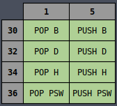
PUSH B
C5
1
SZPC
9
Push value in BC onto the stack
PUSH D
D5
1
SZPC
9
Push value in DE onto the stack
PUSH H
E5
1
SZPC
9
Push value in HL onto the stack
PUSH PSW
F5
1
SZPC
9
Push value in AF onto the stack
POP B
C1
1
SZPC
9
Pop value on stack into BC
POP D
D1
1
SZPC
9
Pop value on stack into DE
POP H
E1
1
SZPC
9
Pop value on stack into HL
POP PSW
F1
1
SZPC
9
Pop value on stack into AF
CALL addr
CD
3
----
16
Call function at addr
CP addr
F4
3
----
4/16
Call function at addr if FlagS == 0
CM addr
FC
3
----
4/16
Call function at addr if FlagS == 1
CNZ addr
C4
3
----
4/16
Call function at addr if FlagZ == 0
CZ addr
CC
3
----
4/16
Call function at addr if FlagZ == 1
CPO addr
E4
3
----
4/16
Call function at addr if FlagP == 0
CPE addr
EC
3
----
4/16
Call function at addr if FlagP == 1
CNC addr
D4
3
----
4/16
Call function at addr if FlagC == 0
CC addr
DC
3
----
4/16
Call function at addr if FlagC == 1
RET
C9
1
----
4
Return from function
RP
F0
1
----
4/10
Return from function if FlagS == 0
RM
F8
1
----
4/10
Return from function if FlagS == 1
RNZ
C0
1
----
4/10
Return from function if FlagZ == 0
RZ
C8
1
----
4/10
Return from function if FlagZ == 1
RPO
E0
1
----
4/10
Return from function if FlagP == 0
RPE
E8
1
----
4/10
Return from function if FlagP == 1
RNC
D0
1
----
4/10
Return from function if FlagC == 0
RC
D8
1
----
4/10
Return from function if FlagC == 1
JMP addr
C3
3
----
4
Jump to addr
JP addr
F2
3
----
4/9
Jump to addr if FlagS == 0
JM addr
FA
3
----
4/9
Jump to addr if FlagS == 1
JNZ addr
C2
3
----
4/9
Jump to addr if FlagZ == 0
JZ addr
CA
3
----
4/9
Jump to addr if FlagZ == 1
JPO addr
E2
3
----
4/9
Jump to addr if FlagP == 0
JPE addr
EA
3
----
4/9
Jump to addr if FlagP == 1
JNC addr
D2
3
----
4/9
Jump to addr if FlagC == 0
JC addr
DA
3
----
4/9
Jump to addr if FlagC == 1
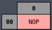
NOP
00
1
----
4
Do nothing
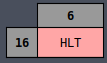
HLT
76
1
----
4
Halt execution
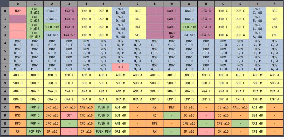
Hexadecimal Table
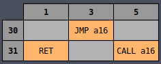
All of the opcodes may look random at first but if you arrange them by their opcodes then it begins
to make a little more sense:
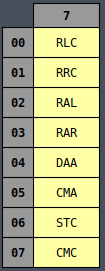
It’s clear from the color coding that there’s definitely a designed ordering to all of the
instructions such that similar instructions are (mostly) laid out near each other. But it still
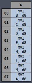
seems slightly random. Why are half of the MVI instructions on the left side and the other half
on the right side? Why are INR and DCR split in half but still next to each other?
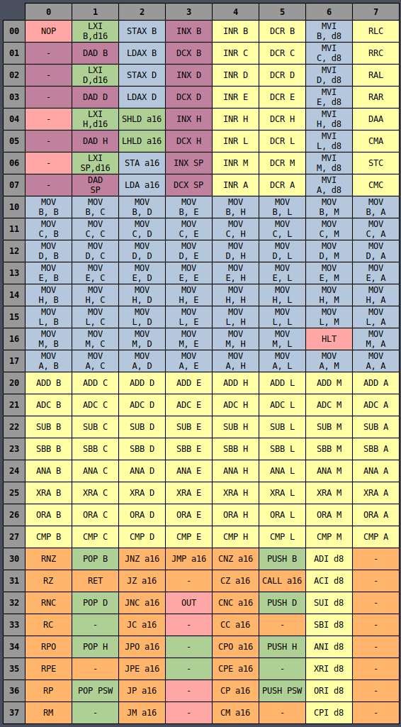
Octal Table
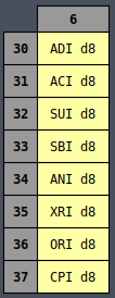
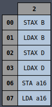
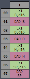
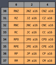
It all becomes much more clear if you instead view the table in octal representation:
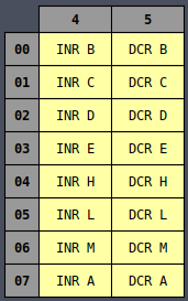
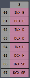
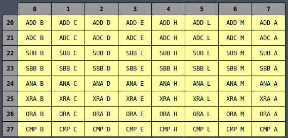
Now all of the MVI instructions are in a single column and the same is true for INR,
DCR, and many others, whether they’re sorted by column or row. There is an underlying logic to
all of the opcodes which is very useful later on for wiring up the controller logic.
Instruction Decoding
The way the decoding works is that different bits of the opcodes mean different things depending on
the type of instruction being decoded. The pattern to the bits makes it easier to decode them into
control signals. Rather than doing checks against every single opcode and then setting the required
signals by hand (like was done for SAP-1 and SAP-2), instead we can pull bits out of the opcode and
connect them to signals without needing to care what the bits actually are.
In a Verilog casez statement, you can specify certain bits as Don’t Care (?) which means
that the case statement will match any bit pattern satisfying the other bits while not caring if the
? bits match or not. For example, the 8-bit octal pattern 8’o1?6 will match: 8’o106, 8’o116,
8’o126, 8’o136, 8’o146, 8’o156, 8’o166, and 8’o176.
Case statements listed earlier will override those listed later, so if you first have 8’o1?6 and
then later 8’o1??, the first will match before the second, allowing it override specific cases
you care about.
There are probably smarter ways of condensing the case statements even further based on the
encoding, but I didn’t want to go so far with it that it became hard to read them.
The first three stages are always the same: grab the next instruction from memory and write it into
the program counter. Then stages four and beyond do different things depending on the instruction.
The framework for the instruction decoding in the controller looks like this:
From here I’ll explain the way each set of related instructions are decoded and show how they map to
Verilog.
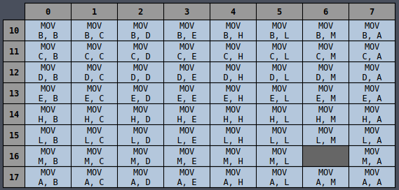
MOV Rd, Rs
Pattern: 8’o1??
opcode[5:3] - Rd
000 - B
001 - C
010 - D
011 - E
100 - H
101 - L
110 - M
111 - A
opcode[2:0] - Rs
000 - B
001 - C
010 - D
011 - E
100 - H
101 - L
110 - M
111 - A
The control signals are different when the source or destination register is M, so they have
their own separate cases that come first to override the later general case.
The control signals are different when the destination register is M, so it has its own separate
case that come first to override the later general case.
// Arithmetic/Logic Set 0 (M)
// opcode[5:3] - ALU Op
8'o2?6:beginif(stage==3)beginctrl_word[REG_RD_SEL4:REG_RD_SEL0]=REG_HL;ctrl_word[REG_OE]=1'b1;ctrl_word[MEM_MAR_WE]=1'b1;endelseif(stage==4)beginctrl_word[MEM_OE]=1'b1;ctrl_word[ALU_TMP_WE]=1'b1;endelseif(stage==5)beginctrl_word[ALU_CS]=1'b1;ctrl_word[ALU_OP4:ALU_OP0]={2'b0,opcode[5:3]};stage_rst=1'b1;endend// Arithmetic/Logic Set 0
// opcode[2:0] - Rs
// opcode[5:3] - ALU Op
8'o2??:beginif(stage==3)beginif(opcode[2:0]==3'b111)beginctrl_word[ALU_CS]=1'b1;ctrl_word[ALU_OP4:ALU_OP0]={2'b0,opcode[5:3]};stage_rst=1'b1;endelsebeginctrl_word[REG_RD_SEL4:REG_RD_SEL0]={2'b0,opcode[2:0]};ctrl_word[REG_OE]=1'b1;endctrl_word[ALU_TMP_WE]=1'b1;endelseif(stage==4)beginctrl_word[ALU_CS]=1'b1;ctrl_word[ALU_OP4:ALU_OP0]={2'b0,opcode[5:3]};stage_rst=1'b1;endend
ALU Secondary
Pattern: 8’o0?7
opcode[5:4]
000 - RLC
001 - RRC
010 - RAL
011 - RAR
100 - DAA
101 - CMA
110 - STC
111 - CMC
1
2
3
4
5
6
7
8
9
// Arithmetic/Logic Set 1
// opcode[5:3] - ALU Op
8'o0?7:beginif(stage==3)beginctrl_word[ALU_CS]=1'b1;ctrl_word[ALU_OP4:ALU_OP0]={2'b01,opcode[5:3]};stage_rst=1'b1;endend
ALU Immediate
Pattern: 8’o3?6
opcode[5:4]
000 - ADI
001 - ACI
010 - SUI
011 - SBI
100 - ANI
101 - XRI
110 - ORI
111 - CPI
 1
 2
 3
 4
 5
 6
 7
 8
 9
10
11
12
13
14
15
16
17
18
// Arithmetic/Logic Immediate
// opcode[5:3] - ALU Op
8'o3?6:beginif(stage==3)beginctrl_word[REG_RD_SEL4:REG_RD_SEL0]=REG_PC;ctrl_word[REG_OE]=1'b1;ctrl_word[MEM_MAR_WE]=1'b1;endelseif(stage==4)beginctrl_word[MEM_OE]=1'b1;ctrl_word[ALU_TMP_WE]=1'b1;endelseif(stage==5)beginctrl_word[ALU_CS]=1'b1;ctrl_word[ALU_OP4:ALU_OP0]={2'b0,opcode[5:3]};ctrl_word[REG_WR_SEL4:REG_WR_SEL0]=REG_PC;ctrl_word[REG_EXT1:REG_EXT0]=REG_INC;stage_rst=1'b1;endend
// OUT
8'o323:beginif(stage==3)beginctrl_word[REG_WR_SEL4:REG_WR_SEL0]=REG_PC;ctrl_word[REG_EXT1:REG_EXT0]=REG_INC;ctrl_word[DISPLAY]=1'b1;stage_rst=1'b1;endend
Results
To prove that things are working as expected, I wrote a simple program that exercises many (but not
all) of the instructions. I tested all of the instructions individually in simulation, but it would
be difficult to write a program that used every instruction. Or at least I can’t think of one.
It uses the stack, jumps around unconditionally and conditionally, calls some functions
unconditionally and conditionally, moves data around registers, uses immediate mode, and does some ALU operations. A nice
variety of instructions (but not all).
The SAP-3 is opcode-compatible with the 8085 so we can use an 8080
Assembler to turn the assembly into machine code.
All assembled it looks like this:
1
2
3
4
5
6
31 f0 00 3e 01 06 00 d3
ff 4f 78 fe 01 79 ca 17
00 c2 20 00 c3 07 00 1f
fe 01 cc 29 00 c3 07 00
17 fe 80 cc 2c 00 c3 07
00 06 00 c9 06 01 c9 76
Behold, the world’s most complicated way to generate a Cylon eye effect:
Source Code
The full unabridged Verilog code can be found
here.